什么是JESD204?我们为何要关注它?
2012年08月02日 14:25 发布者:李宽
一个新的转换器接口正在冉冉升起,期待它会成为未来转换器的首选协议。JESD204是几年前推出的新接口,但经过修改,成为一个更具吸引力和高效的转换接口。由于转换器的分辨率和速度有所提高,对更高效的接口的需求有所增加。JESD204接口带来了高效率。在速度、尺寸和成本方面,它优于它的CMOS和LVDS前辈。采用JESD204的设计具有更快的接口,以保持与更快的采样率转换器的步伐。此外,减少了引脚数,从而导致更小的封装尺寸和更少的跟踪路线,使电路板设计更加容易,并提供更低的整体系统成本。该标准也易于扩展,因此它可以适应未来的需求。这在标准的两次修订中已经体现出来。自2006年推出以来JESD204标准已经经历了两个版本,现在是修订版B。
随着该标准被越来越多的转换器供应商、用户以及FPGA制造商接受,它已得到改进并加入新功能,效率得以提高而且便于实施。本标准适用于模拟到数字转换器(ADC)以及数字模拟转换器(DAC),主要是作为一个到FPGA的通用接口(但也可以用于ASIC)。
JESD204 - 这是什么?
JESD204原始版本在2006年4月发布。该标准描述转换器与接收器之间的(如FPGA或ASIC)的多千兆位串行数据链路。在这JESD204原始版本,串行数据链路被定义为一个单个转换器或多个转换器和一个接收器之间的串行车道。
如图1所示。所示的车道是M个转换器和接收器之间的物理接口,其中包括利用电流模式逻辑(CML)驱动器和接收器的差分互连对。所示的链接是转换器和接收器之间串行数据链。帧时钟路由到转换器和接收器,并提供设备之间的JESD204链接时钟。
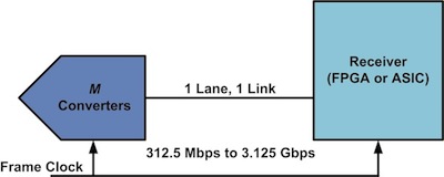
图1. JESD204原始标准
The lane data rate is defined between 312.5 Megabits per second (Mbps) and 3.125 Gigabits per second (Gbps) with both source and load impedance defined as 100 Ω ±20%. The differential voltage level is defined as being nominally 800 mV peak-to-peak with a common mode voltage level range from 0.72 V to 1.23 V. The link utilizes 8b/10b encoding which incorporates an embedded clock, removing the necessity for routing an additional clock line and the associated complexity of aligning an additional clock signal with the transmitted data a high data rates. It became obvious as the JESD204 standard began being used that the standard needed to be revised to incorporate support for multiple aligned serial lanes with multiple converters to accommodate increasing speeds and resolutions of converters.
This realization led to the first revision of the JESD204 standard in April of 2008 which became known as JESD204A. This revision of the standard added the ability to support multiple aligned serial lanes with multiple converters. The lane data rates, supporting from 312.5 Mbps up to 3.125 Gbps remained unchanged as did the frame clock and the electrical interface specifications. Increasing the capabilities of the standard to support multiple aligned serial lanes made it possible for converters with high sample rates and high resolutions to meet the maximum supported data rate of 3.125 Gbps. Figure 2 shows a graphical representation of the additional capabilities added in the JESD204A revision to support multiple lanes.

Figure 2. First Revision – JESD204A
Although both the original JESD204 standard and the revised JESD204A standard were higher performance than legacy interfaces, they were still lacking a key element. This missing element was deterministic latency in the serialized data on the link.
When dealing with a converter, it is important to know the timing relationship between the sampled signal and its digital representation in order to properly recreate the sampled signal in the analog domain once the signal has been received (this situation is, of course for an ADC, a similar situation is true for a DAC). This timing relationship is affected by the latency of the converter which is defined for an ADC as the number of clock cycles between the instant of the sampling edge of the input signal until the time that its digital representation is present at the converter’s outputs. Similarly, in a DAC, the latency is defined as the number of clock cycles between the time the digital signal is clocked into the DAC until the analog output begins changing. In the JESD204 and JESD204A standards, there were no defined capabilities that would deterministically set the latency of the converter and its serialized digital inputs/outputs.
In addition, converters were continuing to increase in both speed and resolution. These factors led to the introduction of the second revision of the standard, JESD204B. In July of 2011, the second and current revision of the standard, JESD204B, was released. One of the key components of the revised standard was the addition of provisions to achieve deterministic latency. In addition, the data rates supported were pushed up to 12.5 Gbps broken down into different speed grades of devices. This revision of the standard calls for the transition from using the frame clock as the main clock source to using the device clock as the main clock source. Figure 3 gives a representation of the additional capabilities added by the JESD204B revision.

Figure 3. Second (Current) Revision – JESD204B
In the previous two versions of the JESD204 standard, there were no provisions defined to ensure deterministic latency through the interface. The JESD204B revision remedies this issue by providing a mechanism to ensure that, from power-up cycle to power-up cycle and across link re-synchronization events, the latency should be repeatable and deterministic. One way this is accomplished is by initiating the initial lane alignment sequence in the converter(s) simultaneously across all lanes at a well-defined moment in time by using an input signal called SYNC~.
Another implementation is to use the SYSREF signal which is a newly defined signal for JESD204B. The SYSREF signal acts as the master timing reference and aligns all the internal dividers from device clocks as well as the local multi-frame clocks in each transmitter and receiver. This helps to ensure deterministic latency through the system. The JESD204B specification calls out three device sub-classes: Sub-class 0 – No support for deterministic latency, Sub-class 1 – Deterministic latency using SYSREF, and Sub-class 2 – Deterministic latency using SYNC~. Sub-class 0 can simply be compared to a JESD204A link. Sub-class 1 is primarily intended for converters operating at or above 500MSPS while Sub-class 2 is primarily for converters operating below 500MSPS.
In addition to the deterministic latency, the JESD204B version increases the supported lane data rates to 12.5 Gbps and divides devices into three different speed grades. The source and load impedance is the same for all three speed grades being defined as 100 Ω ±20%. The first speed grade aligns with the lane data rates from the JESD204 and JESD204A versions of the standard and defines the electrical interface for lane data rates up to 3.125 Gbps. The second speed grade in JESD204B defines the electrical interface for lane data rates up to 6.375 Gbps. This speed grade lowers the minimum differential voltage level to 400 mV peak-to-peak, down from 500 mV peak-to-peak for the first speed grade. The third speed grade in JESD204B defines the electrical interface for lane data rates up to 12.5 Gbps. This speed grade lowers the minimum differential voltage level required for the electrical interface to 360 mV peak-to-peak. As the lane data rates increase for the speed grades, the minimum required differential voltage level is reduced to make physical implementation easier by reducing required slew rates in the drivers.
To allow for more flexibility, the JESD204B revision transitions from the frame clock to the device clock. Previously, in the JESD204 and JESD204A revisions, the frame clock was the absolute timing reference in the JESD204 system. Typically, the frame clock and the sampling clock of the converter(s) were usually the same. This did not offer a lot of flexibility and could cause undesired complexity in system design when attempting to route this same signal to multiple devices and account for any skew between the different routing paths. In JESD204B, the device clock is the timing reference for each element in the JESD204 system. Each converter and receiver receives their respective device clock from a clock generator circuit which is responsible for generating all device clocks from a common source. This allows for more flexibility in the system design, but it requires that the relationship between the frame clock and device clock be specified for a given device.
JESD204 – Why Should We Pay Attention to It?
In much the same way as LVDS began overtaking CMOS as the technology of choice for the converter digital interface several years ago, JESD204 is poised to tread a similar path in the next few years. While CMOS technology is still hanging around today, it is mostly been overtaken by LVDS. The speed and resolution of converters as well as the desire for lower power eventually renders CMOS and LVDS inadequate for converters. As the data rate increases on the CMOS outputs, the transient currents also increase and result in higher power consumption. While the current, and thus power consumption, remains relatively flat for LVDS, the interface has an upper speed bound that it can support. This is due to the driver architecture as well as the numerous data lines that must all be synchronized to a data clock. Figure 4 illustrates the different power consumption requirements of CMOS, LVDS, and CML outputs for a dual 14-bit ADC.

Figure 4. CMOS, LVDS, and CML Driver Power Comparison
At approximately 150 – 200 MSPS and 14 bits of resolution, CML output drivers start to become more efficient in terms of power consumption. CML offers the advantage of requiring fewer output pairs per a given resolution than LVDS and CMOS drivers due to the serialization of the data. The CML drivers specified for the JESD204B interface have an additional advantage since the specification calls for reduced peak to peak voltage levels as the sample rate increases and pushes up the output line rate. The number of pins required for the same give converter resolution and sample rate is also considerably less. Table 1 gives an illustration of the pin counts for the three different interfaces using a 200 MSPS converter with various channel counts and bit resolutions. The data assumes a synchronization clock for each channel’s data in the case of the CMOS and LVDS outputs and a maximum data rate of 4.0 Gbps for JESD204B data transfer using the CML outputs. The reasons for the progression to JESD204B using CML drivers become obvious when looking at this table and observing the dramatic reduction in pin count that can be achieved.
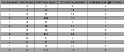
Table 1. Pin Count Comparison – 200 MSPS ADC (click on figure for PDF of the table)
We have seen the trend that is pushing the converter digital interface towards the JESD204 interface defined by JEDEC. Our company has been involved with the standard from the beginning when the first JESD204 specification was released. To date, Analog Devices has released to production several converters with the JESD204 and JESD204A compatible outputs and is currently developing products with outputs that are compatible with JESD204B.
Summary
As the speed and resolution of converters have increased, the demand for a more efficient digital interface has increased as well. The industry began realizing this with the JESD204 serialized data interface. The interface specification has continued to evolve to offer a better and faster way to transmit data between converters and FPGAs (or ASICs). The interface has undergone two revisions to improve upon its implementation and meet the increasing demands brought on by higher speeds and higher resolution converters. Looking to the future of converter digital interfaces, it is clear that JESD204 is poised to become the industry choice for the digital interface to converters. Each revision has answered the demands for improvements on its implementation and has allowed the standard to evolve to meet new requirements brought on by changes in converter technology. As system designs become more complex and converter performance pushes higher, the JESD204 standard should be able to adapt and evolve to continue to meet the new design requirements necessary.
References
JEDEC Standard JESD204 (April 2006). JEDEC Solid State Technology Association. www.jedec.org
JEDEC Standard JESD204A (April 2008). JEDEC Solid State Technology Association. www.jedec.org
JEDEC Standard JESD204B (July 2011). JEDEC Solid State Technology Association. www.jedec.org
About the Author
Jonathan Harris is a product applications engineer, High-Speed Converter Group, Analog Devices, Inc. (Greensboro, NC). He has over 7 years of experience as an applications engineer supporting products in the RF industry. Jonathan received his MSEE from Auburn University and his BSEE from UNC-Charlotte.