On Semi NCV890101汽车级高频降压转换器解决方案
2012年05月22日 12:31 发布者:1770309616
On Semi公司的NCV890101是固定频率降压转换器,内部集成了N沟功率开关,输入电压低至4.5V,高达36V,输出电压可调低至0.8V,误差+/-1.75%,固定工作频率2MHz,峰值电流1.4A,主要用在音频,信息娱乐系统,仪表和安全视觉系统.本文介绍了NCV890101主要特性,方框图,典型应用电路以及评估板NCV890101GEVB主要特性,电路图,材料清单和PCB布局图.The NCV890101 is a fixed−frequency, monolithic, Buck switching regulator intended for Automotive, battery−connected applications that must operate with up to a 36V input supply. The regulator is suitable for systems with low noise and small form factor requirements often encountered in automotive driver information systems.The NCV890101 is capable of converting the typical 4.5 V to 18 V automotive input voltage range to outputs as low as 3.3 V at a constant switching frequency above the sensitive AM band, eliminating the need for costly filters and EMI countermeasures. Two pins are provided to synchronize switching to a clock, or to another NCV890101. The NCV890101 also provides several protection features expected in Automotive power supply systems such as current limit, short circuit protection, and thermal shutdown. In addition, the high switching frequency produces low output voltage ripple even when using small inductor values and an all−ceramic output filter capacitor − forming a space−efficient switching regulator solution.
NCV890101主要特性:
Internal N−Channel Power Switch
Low VIN Operation Down to 4.5 V
High VIN Operation to 36 V
Withstands Load Dump to 40 V
2 MHz Free−running Switching Frequency
Auto−synchronizes with Other NCV890101 or to an External Clock
Logic level Enable Input Can be Directly Tied to Battery
1.4 A (min) Cycle−by−Cycle Peak Current Limit
Short Circuit Protection enhanced by Frequency Foldback
+/-1.75% Output Voltage Tolerance
Output Voltage Adjustable Down to 0.8 V
1.4 Millisecond Internal Soft−Start
Thermal Shutdown (TSD)
Low Shutdown Current
NCV Prefix for Automotive and Other Applications Requiring Site and Change Controls
Wettable Flanks DFN
pb−Free Packages are Available
NCV890101应用:
Audio
Infotainment
Safety − Vision Systems
Instrumentation
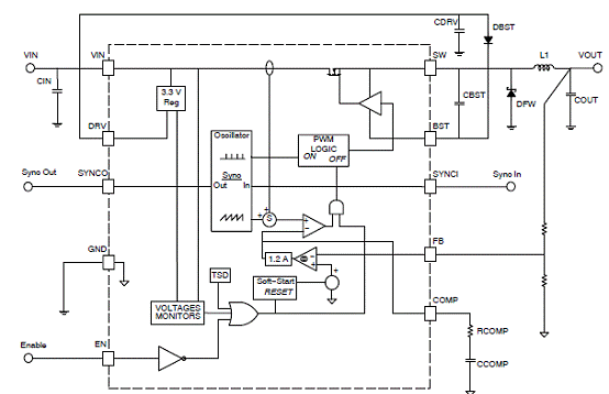
图1.NCV890101方框图
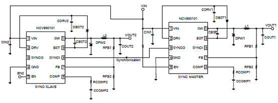
图2.NCV890101同步主从应用电路图:电池使能

图3.NCV890101外时钟同步应用电路图: 电池使能
NCV890101汽车级高频降压转换器评估板NCV890101GEVB
The NCV890101 demonstration board provides a convenient way to evaluate a high-frequency buck converter design. No additional components are required, other than dc supplies for the input and enable voltages. An external clock can be used to synchronize the switching frequency; and the board also provides a synchronization output, enabling it to be used as a master. It is configured for a 3.3 V output with a 2 MHz switching frequency and a 1.2 A maximum output current, over the typical 4.5 V to 18 V automotive input voltage range. In addition, the board regulates up to 36 V thanks to switching frequency foldback.
评估板NCV890101GEVB主要特性:
• 3.3 V Output Voltage
• 2 MHz Switching Frequency
• 1.2 A Current Limit
• Wide Input Voltage of 4.5 V to 36 V
• Regulates through Load Dump Conditions
• External Clock Synchronization up to 2.5 MHz
• Synchronization Output
• Automotive Grade
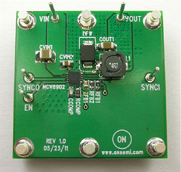
图4. 评估板NCV890101GEVB外形图
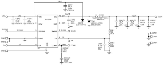
图5. 评估板NCV890101GEVB电路图
评估板NCV890101GEVB材料清单:
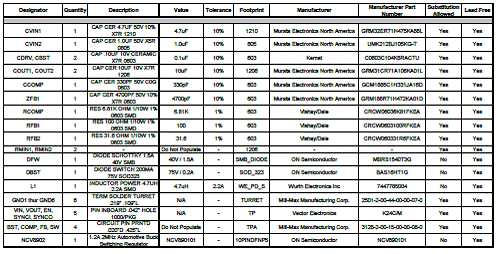
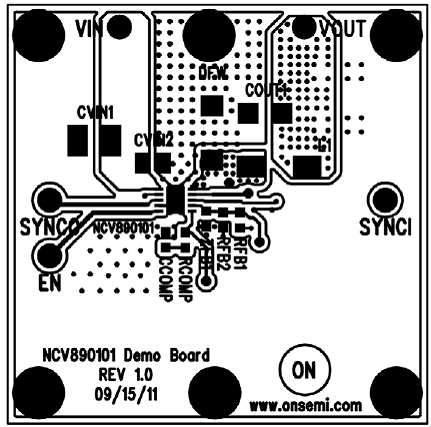
图6. 评估板NCV890101GEVB PCB布局图:顶层
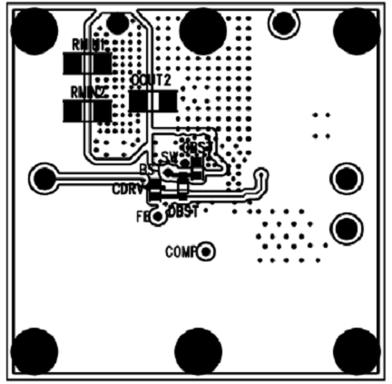
图7. 评估板NCV890101GEVB PCB布局图:底层
详情请见:
77004和
77005
来源:网络
最高输入电压仅36V,有点低。