Linear LTC5569 300MHz-4GHz双路下变换混频方案
2011年12月28日 14:46 发布者:1046235000
Linear公司的LTC5569是300MHz-4GHz频段双路有源下变换混频器,1950MHz时的IIP3为26.8dBm,噪音为11.7dB,变换增益为2dB,通路间隔离为44dB,3.3V的总功耗为600mW,主要用在无线基础设备分集接收器,MIMO接收器和遥控无线电单元.本文介绍了LTC5569主要特性, 方框图, 下变换器测试电路图以及多种应用电路.LTC5569 300MHz to 4GHz 3.3V Dual Active Downconverting Mixer
The LTC®5569 dual active downconverting mixer is optimized for diversity and MIMO receiver applications that require low power and small size. Each mixer includes an independent LO buffer amplifier, active mixer core, and bias circuit with enable pin. The symmetry of the IC assures that a phase and amplitude coherent LO is applied to each mixer.
The RF inputs are 50Ω matched from 1.4GHz to 3.3GHz, and easily matched for higher or lower RF frequencies with simple external matching. The LO input is 50Ω matched from 1GHz to 3.5GHz, even when one or both mixers are disabled. The LO input is easily matched for higher or lower frequencies, as low as 350MHz, with simple external matching. The low capacitance differential IF outputs are usable up to 1.6GHz.
LTC5569主要特性:
High IIP3: 26.8dBm at 1950MHz
2dB Conversion Gain
Low Noise Figure: 11.7dB at 1950MHz
17dB NF Under 5dBm Blocking
44dB Channel Isolation
Low Power: 3.3V/600mW Total
Very Small Solution Size
Enable Pins for Each Mixer
Wide IF Frequency Range
LO Input 50Ω Matched in All Modes
–40℃ to 105℃ Operation
16-Lead (4mm 4mm) QFN package
LTC5569应用:
Wireless Infrastructure Diversity Receivers
MIMO Infrastructure Receivers
Remote Radio Units
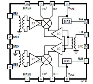
图1. LTC5569方框图
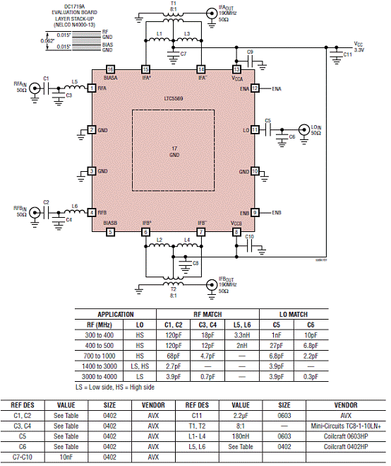
图2. LTC5569下变换器测试电路图(190MHz带通IF匹配)
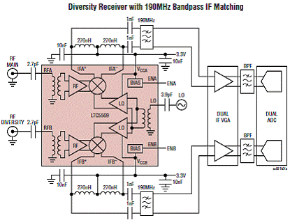
图3. LTC5569 190MHz带通IF匹配分集接收器电路图
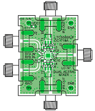
图4. LTC5569评估板布局图
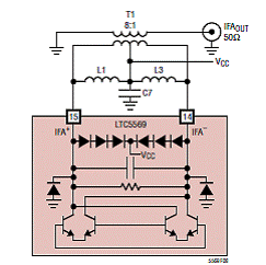
图5. LTC5569带通匹配和8:1变压器的IF输出电路图
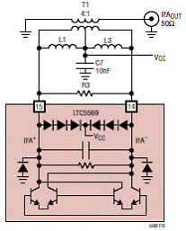
图6. LTC5569宽带匹配和4:1变压器的IF输出电路图
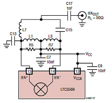
图7. LTC5569分立IF平衡/不平衡变压器匹配电路图
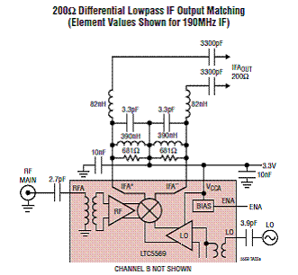
图8. LTC5569 200欧姆差分低通IF输出匹配电路图(所示元件值对应于190MHz IF)
详情请见:
53786