Lattice LatticeECP2 7:1 LVDS视频接口参考设计方案
2011年11月11日 11:10 发布者:1046235000
Lattice公司的LatticeECP2 7:1 LVDS视频评估套件采用LatticeECP2 或LatticeXP2 FPGA,和LatticeECP2高级评估板或LatticeXP2高级评估板以及各种视频I/O源配合使用.本文介绍了LatticeECP2 7:1 接收和发送功能框图, 7:1接收侧和发送侧方框图, LatticeECP2和LatticeXP2 高级评估板的7:1接口测试系统, 视频处理设计案例以及LatticeECP2™高级评估板主要特性,方框图和电路图.The Lattice 7:1 LVDS Video Demo Kit is a set of boards and cables that demonstrate the implementation of a 7:1 LVDS solution using the LatticeECP2 or LatticeXP2 FPGA. The kit works with the LatticeECP2-Advanced Evaluation Board or LatticeXP2 Advanced Evaluation Board, as well as various user video I/O resources.
The default design for use with this kit is based on the 7:1 LVDS Video Interface reference design, targeted for the LatticeECP2 or LatticeXP2 FPGA, and specifically tailored for use with this kit. This, and other resources related to this kit can be downloaded from the links at the left of this page.
7:1 LVDS视频接口包括:
The Lattice 7:1 LVDS Video Demo Kit includes the following:
4 Video Demo Boards (See User Manual for full description - link at left of this page)
LatticeECP2 Advanced Evaluation Board (Optional - see below)
Includes Wall Adapter Power Supply (Universal voltage input, US plugs)
Includes ispDOWNLOAD cable
Banana Jack Cables (For supplying Power to Video Demo Boards from LatticeECP2 Advanced Evaluation Board or other source)
2 Channel-Link MDR Cables
DVI Cable
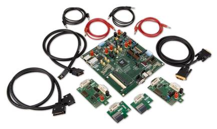
图1. LatticeECP2 7:1 LVDS视频接口评估板外形图
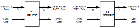
图2. LatticeECP2 7:1 接收和发送功能图
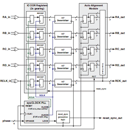
图3.7:1接收侧方框图
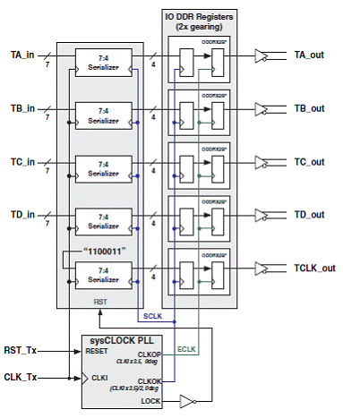
图4.7:1发送侧方框图

图5. LatticeECP2 高级评估板的7:1接口测试系统
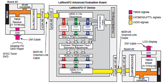
图6. LatticeXP2 高级评估板的7:1接口测试系统
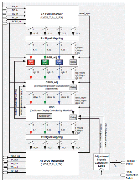
图7.视频处理设计案例
LatticeECP2™高级评估板
The LatticeECP2 Advanced Evaluation Board provides a convenient platform to evaluate, test and debug user designs and IP cores targeted to the LatticeECP2-50 device.
LatticeECP2™高级评估板主要特性:
The main features of this board are listed below:
• LatticeECP2 FPGA with a 1.2V DC core in a 672-ball fpBGA package (default LatticeECP2-50 FPGA)
• SPI Serial Flash device included for low-cost, non-volatile configuration storage
• Two 64-bit DDR2 SO-DIMM module connectors (DDR2 DIMMs are not included)
• VHDM connectors for SPI4.2 transmit and receive interfaces
• Tri-speed (10/100/1000 Mbit) Ethernet PHY that includes RJ-45, magnetics and spark gap
• Directly wired RJ-45 connector
• Samtec TFM-140-31-S-D-LC connector for interfacing with TI DSP motherboards through the peripheral interface
• RS-232 interface chip and 9-pin D-sub connector
• USB 1.1 transceiver and USB type-A and type-B connectors
• Two 8-bit DIP switches
• Discrete LEDs and 7-segment LED
• Compact Flash connector for type I and type II Compact Flash cards (Compact Flash cards not included)
• LCD module connector (LCD module not included)
• Prototyping areas with access to 103 I/O pins
• Selectable I/O bank voltages
• Four pairs of SMA connectors for high speed differential signals
• Oscillator socket for both half-size and full-size oscillators
• 3.3V, 2.5V, 1.8V, 1.2V and ADJ (adjustable voltage) powers generated from a single 5V to 28V power source
• Power Manager ispPAC-POWR1220AT8 chip for monitoring 3.3V, 2.5V, 1.8V, 1.2V, ADJ voltages and DDR VREF,VTTvoltages
• Interface for ispVM System programming support
Also Included:
• 5V/3A AC adapter with international wall plugs
• ispDOWNLOAD Cable (HW-DL-3C or equivalent)
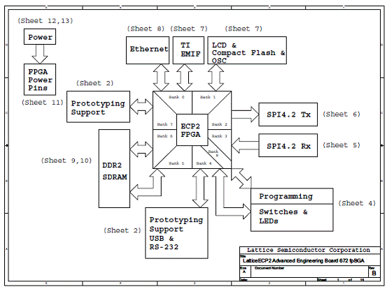
图8.LatticeECP2™高级评估板方框图
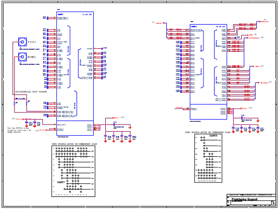
图9.LatticeECP2™高级评估板电路图:支持原型
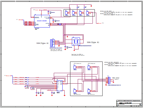
图10.LatticeECP2™高级评估板电路图:USB 1.1和RS-232
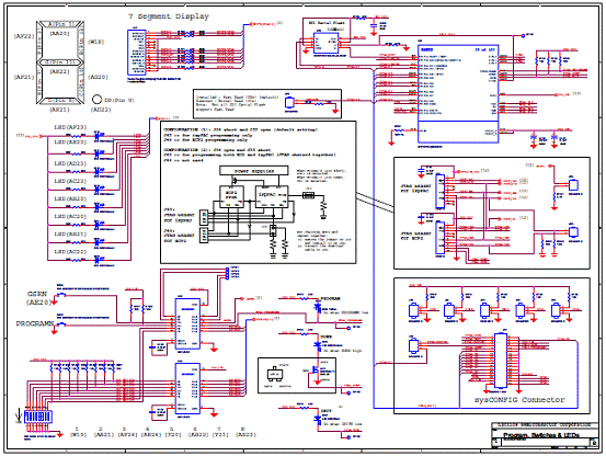
图11.LatticeECP2™高级评估板电路图:编程,开关和LED
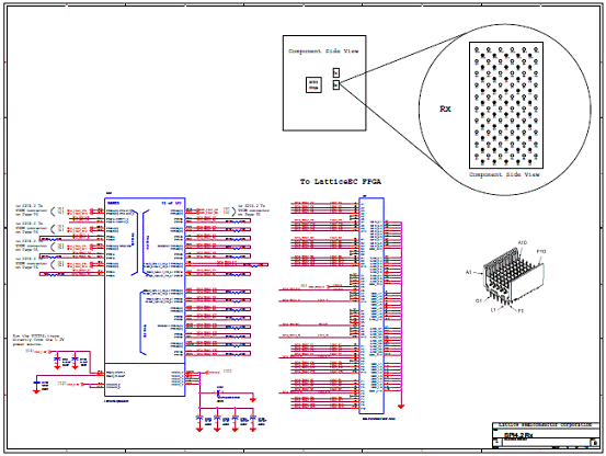
图12.LatticeECP2™高级评估板电路图: SPI4.2 Rx
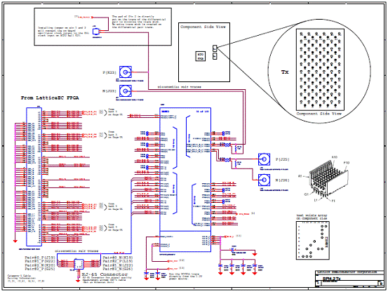
图13.LatticeECP2™高级评估板电路图: SPI4.2 Tx
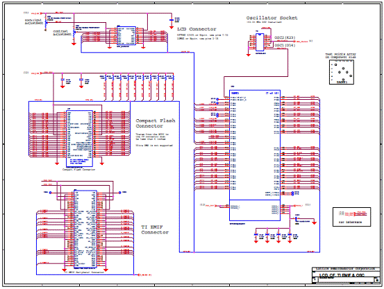
图14.LatticeECP2™高级评估板电路图:LCD, CF, IT EMF和OSC
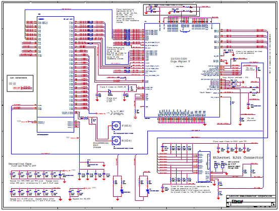
图15.LatticeECP2™高级评估板电路图:以太网
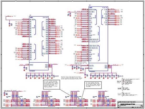
图16.LatticeECP2™高级评估板电路图: DDR2 SDRAM FPGA
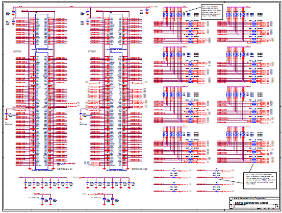
图16.LatticeECP2™高级评估板电路图: DDR2 SDRAM SO-DIMM
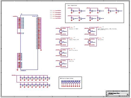
图17.LatticeECP2™高级评估板电路图:FPGA电源引脚
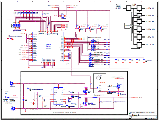
图18.LatticeECP2™高级评估板电路图:电源1
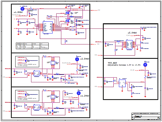
图19.LatticeECP2™高级评估板电路图:电源2
详情请见:
49868和
49867
案