NXP TDF8554J I2CЧЬПЯҝШЦЖ4x45WТфЖө№ҰВК·Еҙу·Ҫ°ё
2011Дк09ФВ24ИХ 22:55 ·ўІјХЯЈә1046235000
NXP№«ЛҫөДTDF8554J КЗјҜіЙБЛ¶аёцөзС№ОИС№ЖчәНБҪёц№ҰВКҝӘ№ШөДI2CЧЬПЯҝШЦЖөД4x45WТфЖө№ҰВК·ЕҙуЖч.·ЕҙуЖчІЙУГ»щУЪSOIөДBCD№ӨТХ,ІЙУГ»ҘІ№өДDMOSКдіцј¶,ҫЯУРҙуКдіцРЕәЕәННкГАөДЙщТфЦКБҝ.Жчјю№ӨЧчөзС№ҝЙөНЦБ6V,I2CЧЬПЯДЈКҪ(3.3VәН5VјжИЭ),ДЬЗэ¶Ҝ2Е·Д·»т4Е·Д·ёәФШ,СпЙщЖч№КХПјмІв,ҝЙұаіМФцТж (26 dBәН16 dB),ЦчТӘУГФЪЖыіөТфЖөПөНі.ұҫОДҪйЙЬБЛTDF8554J ЦчТӘМШРФәНУЕКЖ,·ҪҝтНј, өШПЯЛрәДәНVPЛрәДІвБҝөзВ·Нј,ТФј°ІвБҝәНУҰУГөзВ·НјУлPCBФӘјюІјҫЦНј.The TDF8554J is one of a new generation of complementary quad Bridge-Tied Load (BTL) audio power amplifiers with full I2C-bus controlled diagnostics, multiple voltage regulator and two power switches intended for automotive applications.
The TDF8554J can operate at a battery voltage as low as 6 V making this amplifier suitable for stop/start-car operation. The amplifier uses a complementary DMOS output stage in a Silicon-On-Insulator (SOI)-based BCD process. The DMOS output stage ensures a high power output signal with perfect sound quality. The SOI-based BCD process ensures a robust amplifier, where latch-up cannot occur, with good separation between the four independent channels with every component isolated and without substrate currents.
The multiple voltage regulator comprises four programmable voltage regulators, one standby regulator and two power switches.
The TDF8554J is soft- and hardware downwards-compatible with its predecessor TDA8589XJ.
The TDF8554J includes features, such as selectable undervoltage for stop/start-cars which can be selected with additional I2C-bus instruction bytes. If these additional bytes are not sent, the TDF8554J has the same functionality as its predecessor IPAS TDA8589XJ.
TDF8554J ЦчТӘМШРФәНУЕКЖ:
Amplifier
Stop/start-car prepared: keeps operating without audible disturbance during engine start at a battery voltage as low as 6 V
I2C-bus mode (3.3 V and 5 V compliant)
Can drive 2 ohm or 4ohm loads
Speaker fault detection
Start-up diagnostics with load detection: open, short, present; filtered for door-slam and chatter relays
AC load (tweeter) detection with low and high current mode
Gain select after start-up without audible disturbance
Programmable gain (26 dB and 16 dB), independently programmable for the front and rear channels
Line driver mode (16 dB and mid-tap voltage 0.25VP for stop/start-cars)
Programmable clip detection: 2 %, 5 % or 10 %
Programmable thermal pre-warning
If the temperature protection of the regulator is activated, the amplifier is muted before the regulator is switched off
Loss of ground and open VP safe (with 150 m series impedance and a maximum supply decoupling capacitor of 2200 F)
All amplifier outputs short-circuit proof to ground, supply voltage and across the load (channel independent)
All pins short-circuit proof to ground
Temperature-controlled gain reduction to prevent audio holes at high junction Temperatures
Programmable low battery voltage detection to enable 7.5 V or 6 V minimum battery voltage operation
Overvoltage protection (load-dump safe up to VP = 50 V) and overvoltage pre-warning at 16 V
Offset detection
Multiple regulator
Good stability for any regulator with almost any output capacitor
Five voltage regulators (microcontroller, display, audio processor, mechanical digital and mechanical drive)
I2C-bus controlled
Selectable output voltages for regulators 1, 4 and 5
Low dropout voltage PNP output stages
High supply voltage ripple rejection
Low noise for all regulators
Two power switches (antenna switch and amplifier switch)
Standby regulator (microcontroller supply) operational during load dump and thermal shut-down
Low standby quiescent current (only regulator 2 operational)
Backup functionality for regulator 2
Protection
If connection to the battery voltage is reversed, all regulator voltages will be zero
Able to withstand output voltages up to 18 V if supply line is short-circuited
Thermal protection to avoid thermal breakdown
Load-dump protection
Regulator outputs protected from DC short-circuit to ground or to supply voltage
All regulators protected by foldback current limiting
Power switches protected from loss-of-ground
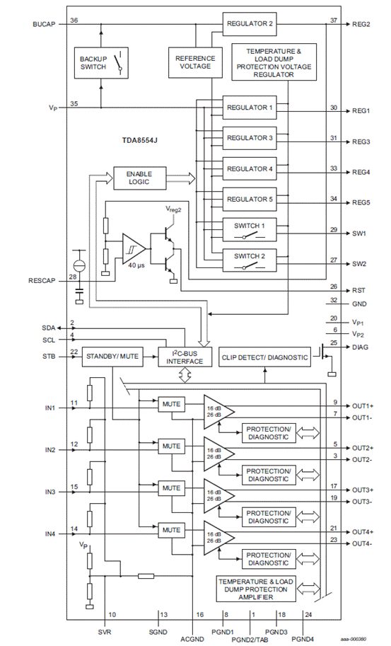
Нј1. TDF8554J·ҪҝтНј
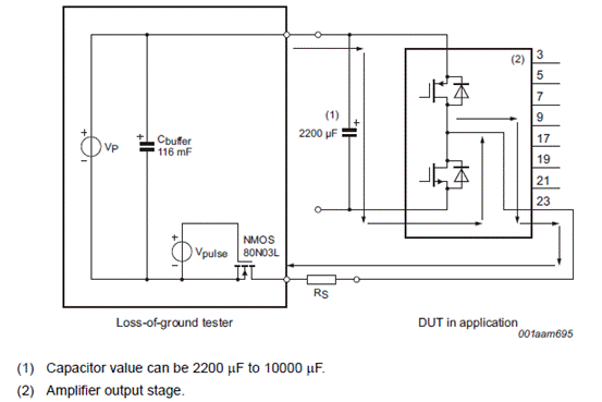
Нј2. TDF8554JөШПЯЛрәДІвБҝөзВ·Нј
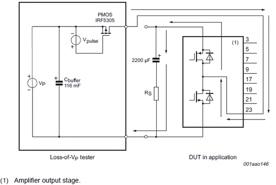
Нј2. TDF8554J VPЛрәДІвБҝөзВ·Нј

Нј4. TDF8554JІвБҝәНУҰУГөзВ·Нј
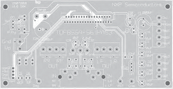
Нј5. TDF8554J PCBФӘјюІјҫЦНј(¶ҘІг)
ПкЗйЗлјы:
45351