ADI ADN2812 评估板参考设计方案
2012年10月27日 11:30 发布者:1770309616
ADN2812是ADI公司生产的一款具有量化接收机功能,信号电平检测、时钟和数据恢复功能,连续数据率从12.3Mb/s到2.7Gb/s。ADN2812芯片在没有外部基准时钟或编程的情况下,自动锁存所有数据速率。满足所有光纤网络抖动,包括抖动转移、抖动生成和抖动公差。本文主要介绍ADN2812的主要特性、方框图及其应用。同时介绍EVAL-ADN2812EB评估板、电路图、材料清单和PCB Layout图。The ADN2812 provides the receiver functions of quantization, signal level detect, and clock and data recovery for continuous data rates from 12.3 Mb/s to 2.7 Gb/s. The ADN2812 auto-matically locks to all data rates without the need for an external reference clock or programming. All SONET jitter requirements are met, including jitter transfer, jitter generation, and jitter tolerance. All specifications are quoted for −40℃ to +85℃ ambient temperature, unless otherwise noted.
This device, together with a PIN diode and a TIA preamplifier, can implement a highly integrated, low cost, low power fiber optic receiver.
The receiver front end, loss of signal (LOS) detector circuit indicates when the input signal level has fallen below a user-adjustable threshold. The LOS detect circuit has hysteresis to prevent chatter at the output.
The ADN2812 is available in a compact 5 mm × 5 mm 32-lead lead frame chip scale package (LFCSP).
ADN2812主要特性:
Serial data input: 12.3 Mb/s to 2.7 Gb/s
Exceeds SONET requirements for jitter transfer/ generation/tolerance
Quantizer sensitivity: 6 mV typical
Adjustable slice level: ±100 mV
Patented clock recovery architecture
Loss of signal (LOS) detect range: 3 mV to 15 mV
Independent slice level adjust and LOS detector
No reference clock required
Loss of lock indicator
I2C interface to access optional features
Single-supply operation: 3.3 V
Low power: 750 mW typical
5 mm × 5 mm 32-lead LFCSP
ADN2812应用:
SONET OC-1/OC-3/OC-12/OC-48 and all associated FEC rates
Fibre Channel, 2× Fibre Channel, GbE, HDTV
WDM transponders
Regenerators/repeaters
Test equipment
Broadband cross-connects and routers
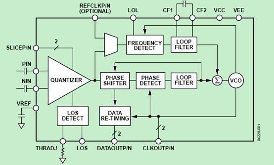
图1. ADN2812方框图
EVAL-ADN2812EB介绍:
This application note describes the use of the EVAL-ADN2812EB. The ADN2812 is a continuous rate clockrecovery, data-retiming device based on a multiloop PLL architecture. The ADN2812 can automatically lock to any data rate from 10 Mbps to 2.7 Gbps, recover the clock, and retime the data without programming and without the need for an external reference clock as an acquisition aid. An I2C“ interface is available to access special features of the ADN2812; however, it is not required for normal operation.
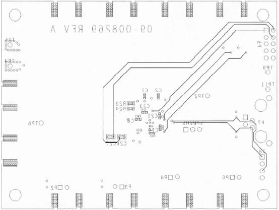
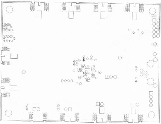
The EVAL-ADN2812EB is fabricated using standard FR-4 materials. All high speed differential signal traces are matched to within 3 mils length and maintain a 50 characteristic impedance to preserve signal integrity.
EVAL-ADN2812EB电路图:
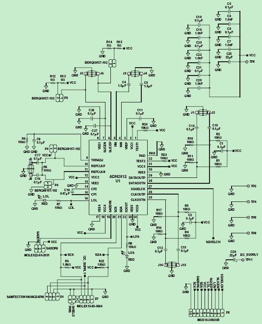
图2. EVAL-ADN2812EB电路图
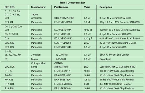
EVAL-ADN2812EB材料清单:
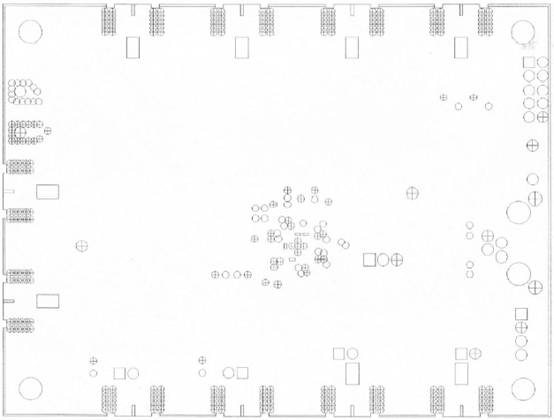
PCB Layout图:

详细资料如下
91377
91378 来源:网络