Avnet ADI ADP1850 Xilinx 7系列FPGA电源解决方案
2012年08月29日 12:07 发布者:1770309616
Avnet公司的ADI电源模块是采用ADI公司的ADP1850 器件,专为Xilinx 公司的7系列FPGA提供电源,12V电压输入,四个双路ADP1850器件提供8路稳压输出:3.3V/8A,2.5V/8A,2.0V/2A,1.8V/6A,1.5V或1.35V/4A,1.2V/4A和两路1.0V/6A.输出误差在3%或5%.本文介绍了ADI电源模块主要指标和特性,方框图,电路图,材料清单和PCB布局图.The Analog Devices Power Module provides a proven robust design for powering Xilinx 7 series devices. Designed to meet the tolerance and sequencing guidelines set forth by Xilinx, the Analog Devices Power Module provides a highly optimized controller based design utilizing the ADP1850 dual output synchronous buck controller. The device operates in current mode for improved transient response and uses valley current sensing for enhanced noise immunity. The ADP1850 is ideal in system applications requiring multiple output voltages: the ADP1850 includes a synchronization feature to eliminate beat frequencies between switching devices; provides accurate tracking capability between supplies and includes precision enable for simple, robust sequencing. The ADP1850 provides high speed, high peak current drive capability with dead-time optimization to enable energy efficient power conversion. For low load operation, the device can be configured to operate in power saving mode (PSM) by skipping pulses and reducing switching losses to improve the energy efficiency at light load and standby conditions.
Additional flexibility is provided by external programmability of loop compensation, soft start, frequency setting, power saving mode, current limit and current sense gain can all be programmed using external components.
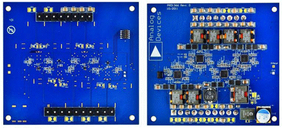
图1.ADI电源模块外形图
ADI电源模块主要指标:

ADI电源模块主要特性:
12 V input
Eight regulated outputs (4 dual output ADP1850 devices)
3.3 V @ 8 A output, 5% tolerance
2.5 V @ 8 A output, 5% tolerance
2.0 V @ 2 A output, 3% tolerance
1.8 V @ 6 A output, 5% tolerance
1.5 V/1.35 V @ 4 A jumper selectable output, 5% tolerance
1.2 V @ 4 A output, 2.5% tolerance
1.0 V @ 6 A output, 3% tolerance
Second 1.0 V @ 6 A output, 3% tolerance
Remote sense for greater regulation accuracy at the load on all outputs
Meets recommended start up sequencing for Xilinx 7 series devices
Vccint -> Vccaux -> Vccaux_io -> Vcco
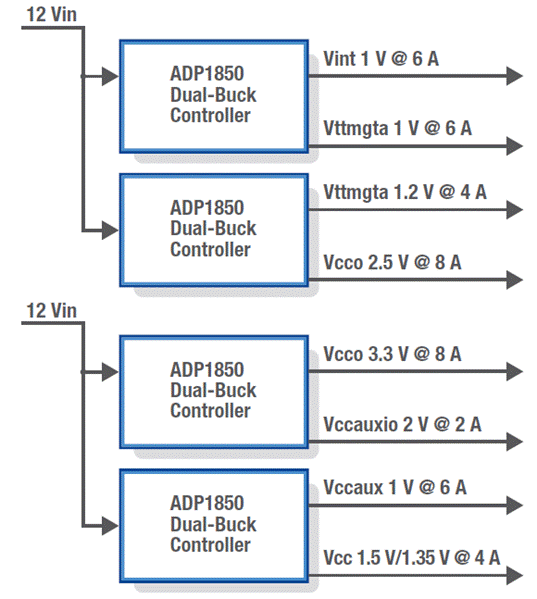
图2.ADI电源模块框图
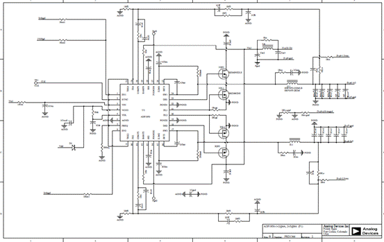
图3.ADI电源模块电路图(1)
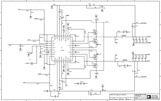
图4.;ADI电源模块电路图(2)
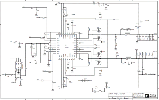
图5.ADI电源模块电路图(3)
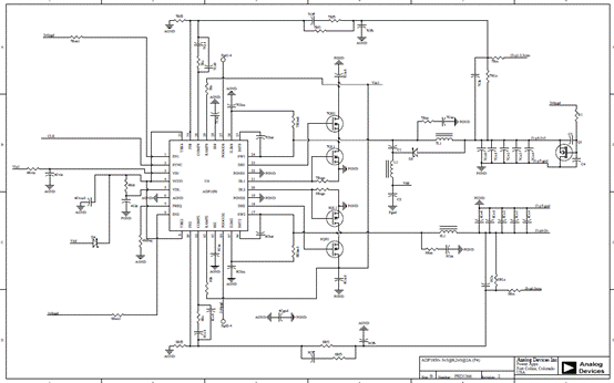
图6.ADI电源模块电路图(4)
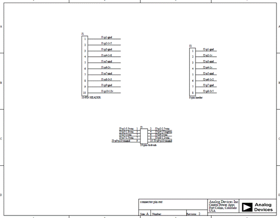
图7.ADI电源模块电路图(4)
ADI电源模块材料清单(BOM)见:

图8.ADI电源模块PCB布局图(顶层)
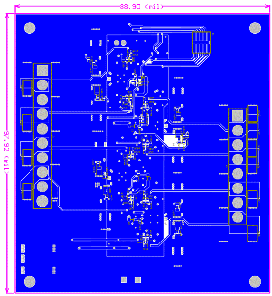
图9.ADI电源模块PCB布局图(底层)
详情请见:
87002
和
https://www.em.avnet.com/Support%20And%20Downloads/ADI%20Power%20Module%20User%20Guide_release%2001.pdf
以及
https://www.em.avnet.com/Support%20And%20Downloads/ADI%20Power%20Module%20Schematic%20R02.pdf
来源:网络
