Cypress CY8C24894����������ϵͳ�������
2011��12��13�� 16:10 �����ߣ�1640190015
Cypress��˾�ij���������ϵͳ����CY8C24894 PSoCϵ������,����ʵ����·���������ϵͳ(���������������κνӽ�����ľ���).���Ľ����˳���������ϵͳ�Ŀ�ͼ�Լ������õ���������CY8C24894��Ҫ����,����ͼ, CY3214-PSoCEVALUSB��������Ҫ����,��ͼ,��·ͼ,�����嵥��PCB����ͼ.Automotive PSoC® Programmable System-on-Chip
The PSoC family consists of many Programmable System-on-Chip with on-chip controller devices. All PSoC family devices are designed to replace traditional microcontroller units(MCUs), system ICs, and the numerous discrete components that surround them. Configurable analog, digital, and interconnect circuitry enable a high level of integration in a host of industrial, consumer, and communication applications.
This architecture allows the user to create customized peripheral configurations that match the requirements of each individual application. Additionally, a fast CPU, Flash program memory, SRAM data memory, and configurable I/O are included in a range of convenient pinouts and packages.
The PSoC architecture is comprised of four main areas: PSoc Core, digital system, analog system, and system resources. Configurable global busing allows all the device resources to be combined into a complete custom system. The PSoC CY8C24x94 devices can have up to seven I/O ports that connect to the global digital and analog interconnects, providing access to four digital blocks and six analog blocks.
The PSoC Core
The PSoC Core is a powerful engine that supports a rich feature set. The core includes a CPU, memory, clocks, and configurable GPIOs.
The M8C CPU core is a powerful processor with speeds up to 24 MHz, providing a four-MIPS 8-bit Harvard architecture microprocessor. The CPU uses an interrupt controller with up to 20 vectors, to simplify programming of real-time embedded events.Program execution is timed and protected using the included sleep timer and watchdog timer (WDT).
Memory encompasses 16 KB of flash for program storage, 1 KB of SRAM for data storage, and up to 2 KB of emulated EEPROM using the flash. Program flash has four protection levels on blocks of 64 bytes, allowing customized software IP protection.
The PSoC device incorporates flexible internal clock generators, including a 24-MHz internal main oscillator (IMO) accurate to ��4% over temperature and voltage. The 24-MHz IMO can also be doubled to 48 MHz for use by the digital system. A low power 32-kHz internal low-speed oscillator (ILO) is provided for the sleep timer and WDT. The clocks, together with programmable clock dividers (as system resources), provide the flexibility to integrate almost any timing requirement into the PSoC device.
PSoC GPIOs provide connection to the CPU, digital resources, and analog resources of the device. Each pin��s drive mode may be selected from eight options, allowing great flexibility in external interfacing. Every pin is also capable of generating a system interrupt.
The Digital System
The digital system is composed of four digital PSoC blocks. Each block is an 8-bit resource used alone or combined with other blocks to form 8-, 16-, 24-, and 32-bit peripherals, which are called user modules.
Digital peripheral configurations include those listed below.
�� PWMs (8- to 32-bit)
�� PWMs with Dead band (8- to 24-bit)
�� Counters (8- to 32-bit)
�� Timers (8- to 32-bit)
�� Full- or half-duplex 8-bit UART with selectable parity
�� SPI master and slave
�� I2C master, slave, or multimaster (implemented in a dedicated I2C block)
�� Cyclic redundancy checker/generator (16-bit)
�� Infrared Data Association (IrDA)
�� PRS generators (8- to 32-bit)
The digital blocks can be connected to any GPIO through a series of global buses that can route any signal to any pin. The buses also allow signal multiplexing and performing logic operations.
This configurability frees your designs from the constraints of a fixed peripheral controller.
Digital blocks are provided in rows of four, where the number of blocks varies by PSoC device family. This allows you the optimum choice of system resources for your application.
The Analog System
The analog system is composed of six configurable blocks, each comprised of an opamp circuit allowing the creation of complex analog signal flows. Analog peripherals are very flexible and can be customized to support specific application requirements.
Some of the more common PSoC analog functions (most available as user modules) are listed below.
�� ADCs (up to two, with 6- to 14-bit resolution, selectable as incremental, delta-sigma, or successive approximation register (SAR))
�� Filters (Two- and Four-pole band pass, low pass, and notch)
�� Amplifiers (up to two, with selectable gain to 48x)
�� Instrumentation amplifiers (one with selectable gain to 93x)
�� Comparators (up to two, with 16 selectable thresholds)
�� DACs (up to two, with 6- to 9-bit resolution)
�� Multiplying DACs (up to two, with 6- to 9-bit resolution)
�� High current output drivers (two with 30 mA drive)
�� 1.3-V reference (as a system resource)
�� DTMF Dialer
�� Modulators
�� Correlators
�� Peak Detectors
�� Many other topologies possible
The Analog Multiplexer System
The analog mux bus can connect to every GPIO pin in ports 0-5. Pins are connected to the bus individually or in any combination.
The bus also connects to the analog system for analysis with comparators and ADCs. It can be split into two sections for simultaneous dual-channel processing. An additional 8:1 analog input multiplexer provides a second path to bring Port 0 pins to the analog array.Switch control logic enables selected pins to precharge continuously under hardware control. This enables capacitive measurement for applications such as touch sensing. Other multiplexer applications include:
�� Track pad, finger sensing.
�� Chip-wide mux that allows analog input from up to 47 I/O pins.
�� Crosspoint connection between any I/O pin combination.
Additional System Resources
System resources provide additional capability useful for complete systems. Additional resources include a multiplier, decimator, LVD, and power-on reset (POR). Brief statements describing the merits of each resource follow.
�� Digital clock dividers provide three customizable clock frequencies for use in applications. The clocks can be routed to both the digital and analog systems. Additional clocks are generated using digital PSoC blocks as clock dividers.
�� Two multiply accumulates (MACs) provide fast 8-bit multipliers with 32-bit accumulate, to assist in both general math and digital filters.
CY8C24894��Ҫ����:
�� Automotive Electronics Council (AEC) qualified
�� Powerful Harvard-architecture processor
❐ M8C processor speeds up to 24 MHz
❐ Two 8 �� 8 multiply, 32-bit accumulate
❐ Low power at high speed
❐ Operating voltage: 3.0 V to 5.25 V
❐ Automotive temperature range: �C40 �� to +85 ��
�� Advanced peripherals (PSoC® blocks)
❐ Six rail-to-rail analog PSoC blocks provide:
• Up to 14-bit analog-to-digital converters (ADCs)
• Up to 9-bit digital-to-analog converters (DACs)
• Programmable gain amplifiers (PGAs)
• Programmable filters and comparators
❐ Four digital PSoC blocks provide:
• 8- to 32-bit timers, counters, and pulse-width modulators (PWMs)
• Cyclic redundancy check (CRC) and pseudo-random sequence (PRS) modules
• Full- or half-duplex UART
• SPI master or slave
• Connectable to all general purpose I/O (GPIO) pins
❐ Complex peripherals by combining blocks
• Capacitive sensing application capability
�� Flexible on-chip memory
❐ 16 KB flash program storage, 1000 erase/write cycles
❐ 1 KB SRAM data storage
❐ In-system serial programming (ISSP)
❐ Partial flash updates
❐ Flexible protection modes
❐ EEPROM emulation in flash
�� Programmable pin configurations
❐ 25 mA sink, 10 mA drive on all GPIOs
❐ Pull-up, pull-down, high Z, strong, or open-drain drive modes on all GPIOs
❐ Up to 47 analog inputs on GPIOs
❐ Two 30 mA analog outputs on GPIOs
❐ Configurable interrupt on all GPIOs
�� Precision, programmable clocking
❐ Internal ��4% 24/48 MHz oscillator
❐ Internal low-speed, low-power oscillator for watchdog and sleep functionality
❐ Optional external oscillator, up to 24 MHz
�� Additional system resources
❐ I2C™ slave, master, or multimaster operation up to 400 kHz
❐ Watchdog and sleep timers
❐ User-configurable LVD
❐ Integrated supervisory circuit
❐ On-chip precision voltage reference
�� Complete development tools
❐ Free development software (PSoC Designer™)
❐ Full-featured in-circuit emulator (ICE) and programmer
❐ Full-speed emulation
❐ Complex breakpoint structure
❐ 128 KB trace memory
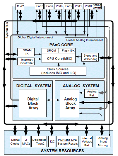
ͼ1.CY8C24894������ͼ
��������������ϵͳ
This figure represents an ultrasonic parking assistance system(UPAS) with the implementation of a four-channel ultrasonic distance measurement system using PSoC. The implementation in the block diagram measures the distance between the ultrasonic transducers and any nearby objects. The system must provide the distance measurement to the rest of the vehicle to be used as desired.
PSoC offers more integration than any standard MCU helping reduce BOM, improve quality and time to market.
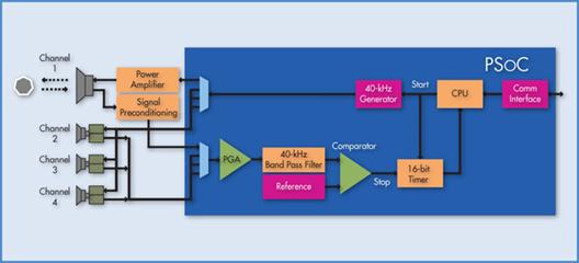
ͼ2.��������������ϵͳ��ͼ
CY3214-PSoCEVALUSB������
The CY3214-PSoCEVALUSB Kit includes a development board for the CY8C24894-24LTXI PSoC® device. Note that the board has the CY8C24094 device, which is an on-chip debug part for the CY8C24x94 family. You can design your own projects with PSoC Designer™ or by altering the code examples provided with this kit. It is a combination of technologies that create opportunities for a new range of low-cost, mixed-signal USB products. This architecture enables creating customized peripheral configurations that match the requirements of individual applications.
The CY3214-PSoCEVALUSB Kit is based on the PSoC 1 family of devices. PSoC is a Programmable System-on-Chip™ platform for 8-bit applications. It combines precision analog and digital logic with a high-performance CPU. With PSoC, you can create the exact combination of peripherals and integrated proprietary IP to meet the needs of your applications.
Chapter 2 describes the installation and configuration of the CY3214-PSoCEVALUSB Kit, PSoC Designer and PSoC Programmer. Chapter 3 describes the kit operation, with the help of the ��Square Mouse�� project, which comes as a demonstration with the CY3214-PSoCEVALUSB kit. It also explains the programming connections of a PSoC 1 device with the PSoC MiniProg and power supply. Chapter 4 describes the hardware operations. Chapter 5 provides the description of the execution of simple projects. The Appendix section provides the schematics and bill of materials (BOM).
CY3214-PSoCEVALUSB����������:
�� PSoCEVALUSB board
�� LCD module
�� MiniProg Programmer
�� USB A to Mini B cable
�� CY3214-PSoCEVALUSB Kit CD
❐ PSoC Designer installation file
❐ PSoC Programmer installation file
❐ Code examples
❐ Hardware files
❐ Kit guide
❐ Quick start guide
❐ Release notes
�� Jumper wire pack
�� CY8C24894-24LTXI sample silicon
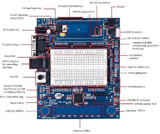
ͼ3. CY3214-PSoCEVALUSB����������ͼ
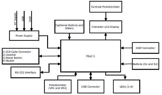
ͼ4. CY3214-PSoCEVALUSB������Ӳ����ͼ

ͼ5. CY3214-PSoCEVALUSB��������·ͼ
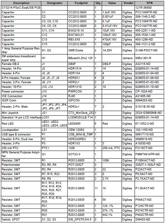
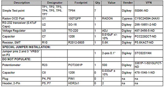
CY3214-PSoCEVALUSB�����������嵥:
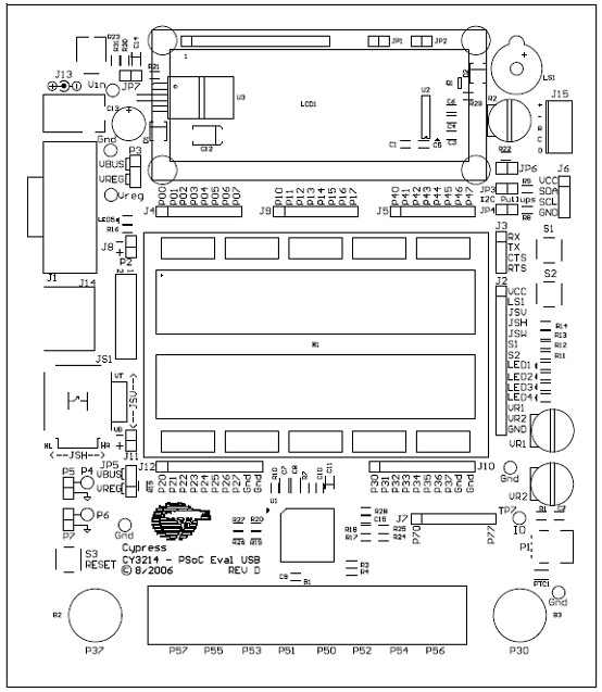
ͼ6. CY3214-PSoCEVALUSB������PCB����ͼ
�������:
52622��
52623