On Semi NCV7425 LIN网络连接解决方案
2011年12月06日 20:53 发布者:Liming
On Semi 公司的NCV7425是全特性局部互连网络(LIN) v2.1收发器,用在LIN协议控制器和物理总线间接口.器件还集成了低压降稳压器.总线电压±45 V,传输速率高达20k波特,输出电压3.3V或5V,负载电流高达150mA,主要用在汽车和工业网络.本文介绍了NCV7425主要特性,功能方框图,应用框图以及评估板NCV74250V1GEVB主要特性,电路图,材料清单和PCB布局图.The NCV7425 is a fully featured local interconnect network (LIN) transceiver designed to interface between a LIN protocol controller and the physical bus.
The NCV7425 LIN device is a member of the in−vehicle networking (IVN) transceiver family of ON Semiconductor that integrates a LIN v2.1 physical transceiver and a low−drop voltage regulator. It is designed to work in harsh automotive environment and is submitted to the TS16949 qualification flow.
The LIN bus is designed to communicate low rate data from control devices such as door locks, mirrors, car seats, and sunroofs at the lowest possible cost. The bus is designed to eliminate as much wiring as possible and is implemented using a single wire in each node. Each node has a slave MCU−state machine that recognizes and translates the instructions specific to that function. The main attraction of the LIN bus is that all the functions are not time critical and usually relate to passenger comfort.
NCV7425主要特性:
• LIN−Bus Transceiver
♦ LIN compliant to specification revision 2.1(backward compatible to versions 2.0 and 1.3) and J2602
♦ Bus Voltage ±45 V
♦ Transmission Rate up to 20 kBaud
♦ Integrated Slope Control for Improved EMI Compatibility
• Package
♦ SOIC−16 Wide Body Green Package with Exposed Pad
• Protection
♦ Thermal Shutdown
♦ Indefinite Short−Circuit Protection on Pins LIN and WAKE Towards Supply and Ground
♦ Load Dump Protection (45 V)
♦ Bus Pins Protected Against Transients in an Automotive Environment
♦ ESD Protection Level for LIN, INH, WAKE and VBB up to ±10 kV
• Voltage Regulator
♦ Two Device Versions: Output Voltage 3.3 V or 5 V For Loads up to 150 mA
♦ Under−Voltage Detector with a Reset Output to the Supplied Microcontroller
♦ INH Output for Auxiliary Purposes (switching of an external pull−up or resistive divider towards battery, control of an external voltage regulator etc.)
• Modes
♦ Normal Mode: LIN Communication in Either Low (up to 10 kBaud) or Normal Slope
♦ Sleep Mode: VCC is Switched “off” and No Communication on LIN Bus
♦ Stand−by Mode: VCC is Switched “on” but There is No Communication on LIN Bus
♦ Wake−up Bringing the Component From Sleep Mode Into Standby Mode is Possible Either by LIN Command or Digital Input Signal on WAKE Pin Wake−up from LIN Bus can also be Detected and Flagged When the Chip is Already in Standby Mode
• Pb−Free Packages are Available
NCV7425典型应用:
• Automotive
• Industrial Networks
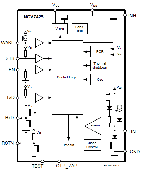
图1.NCV7425功能方框图
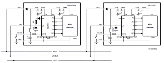
图2.NCV7425应用框图
评估板NCV74250V1GEVB
The NCV74250V1GEVB is a Reference Design for LIN transceiver with integrated low drop voltage regulator. The reference design can be interfaced via IO pins to an external microcontroller or simple switch board. The boards are intended to give designers easy, quick and convenient means for evaluation of NCV7425 devices. The design incorporates the lowest bill of material and small board size.
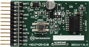
图3.评估板NCV74250V1GEVB外形图
This document describes the NCV7425EVB board for the ON Semiconductor NCV7425 LIN Transceiver with Voltage Regulator and Reset pin. The functionality and major parameters can be evaluated with the NCV7425EVB board.
The NCV7425 is a fully featured local interconnect network (LIN) transceiver designed to interface between a LIN protocol controller and the physical bus.
The NCV7425 LIN device is a member of the in-vehicle networking (IVN) transceiver family of ON Semiconductor that integrates a LIN v2.1 physical transceiver and a low-drop voltage regulator. It is designed to work in harsh automotive environment and is submitted to the TS16949 qualification flow.
评估板NCV74250V1GEVB特性:
One-row Pin Header Connecting to all Circuit Signals Enables Easy Insertion of the Evaluation Board into a more Complex Application Setup.
The Header can be Alternatively Assembled either Perpendicular or Parallel with the Board Plane
Oscilloscope Test-points on All Circuit Signals
Reverse Protection and Decoupling on the Main (Battery) Supply
Decoupling on VCC Regulator Output
Additional Pull-up Resistor on the RSTN Open-drain Output
Filtering Circuit on the Switch-monitoring WAKE Input
On-board Local Wakeup Switch
LIN-bus Termination and Optional ESD Protection
Good Thermal Connection of the Circuit’s Exposed Pad to the Bottom Ground Plane
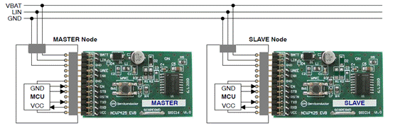
图4.评估板NCV74250V1GEVB建立连接图
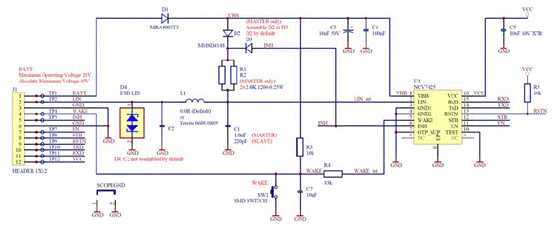
图5.评估板NCV74250V1GEVB电路图
评估板NCV74250V1GEVB材料清单:
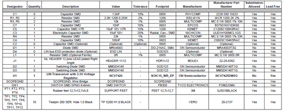
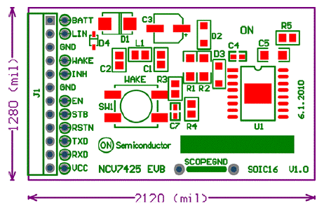
图6.评估板NCV74250V1GEVB PCB布局图
详情请见:
52110和
52109