Microchip dsPIC33F 动力线通Modem(PLM)子板解决方案
2011年09月13日 12:57 发布者:Liming
Microchip公司的dsPIC33FJ06GS101/X02和dsPIC33FJ16GSX02/X04包括了DSP功能和高性能16位MCU架构,在3.0-3.6V时可达40MIPS,多达35个可编数字I/O引脚,闪存多达16KB,集成了高速PWM模块,中断控制器,高速比较器和10位ADC以及多种外设,主要用在动力线通信,包括电表,家庭能量监控和智能电网.本文介绍了dsPIC33F系列产品主要特性,方框图,动力线通信调制解调器(PLM) PICtail+子板框图,电路图材料清单和PCB元件布局图.dsPIC33FJ06GS101/X02 and dsPIC33FJ16GSX02/X04 devices contain extensive Digital Signal Processor (DSP) functionality with a high-performance, 16-bit microcontroller (MCU) architecture.
dsPIC33F主要特性:
Operating Range:
• Up to 40 MIPS Operation (at 3.0-3.6V):
- Industrial temperature range (-40℃ to +85℃)
- Extended temperature range (-40℃ to +125℃)
High-Performance DSC CPU:
• Modified Harvard Architecture
• C Compiler Optimized Instruction Set
• 16-Bit Wide Data Path
• 24-Bit Wide Instructions
• Linear Program Memory Addressing up to 4M Instruction Words
• Linear Data Memory Addressing up to 64 Kbytes
• 83 Base Instructions: Mostly 1 Word/1 Cycle
• Two 40-Bit Accumulators with Rounding and Saturation Options
• Flexible and Powerful Addressing modes:
- Indirect
- Modulo
- Bit-Reversed
• Software Stack
• 16 x 16 Fractional/Integer Multiply Operations
• 32/16 and 16/16 Divide Operations
• Single-Cycle Multiply and Accumulate:
- Accumulator write back for DSP operations
- Dual data fetch
• Up to ±16-Bit Shifts for up to 40-Bit Data
Digital I/O:
• Peripheral Pin Select Functionality
• Up to 35 Programmable Digital I/O Pins
• Wake-up/Interrupt-on-Change for up to 30 Pins
• Output Pins can Drive Voltage from 3.0V to 3.6V
• Up to 5V Output with Open-Drain Configuration
• 5V Tolerant Digital Input Pins (except RB5)
• 16 mA Source/Sink on All PWM pins
On-Chip Flash and SRAM:
• Flash Program Memory (up to 16 Kbytes)
• Data SRAM (up to 2 Kbytes)
• Boot and General Security for Program Flash
Peripheral Features:
• Timer/Counters, up to Three 16-Bit Timers:
- Can pair up to make one 32-bit timer
• Input Capture (up to two channels):
- Capture on up, down or both edges
- 16-bit capture input functions
- 4-deep FIFO on each capture
• Output Compare (up to two channels):
- Single or Dual 16-Bit Compare mode
- 16-Bit Glitchless PWM mode
• 4-Wire SPI:
- Framing supports I/O interface to simple codecs
- 1-deep FIFO Buffer.
- Supports 8-bit and 16-bit data
- Supports all serial clock formats and sampling modes
• I2C™:
- Supports Full Multi-Master Slave mode
- 7-bit and 10-bit addressing
- Bus collision detection and arbitration
- Integrated signal conditioning
- Slave address masking
• UART:
- Interrupt on address bit detect
- Interrupt on UART error
- Wake-up on Start bit from Sleep mode
- 4-character TX and RX FIFO buffers
- LIN bus support
- IrDA® encoding and decoding in hardware
- High-Speed Baud mode
- Hardware Flow Control with CTS and RTS
Interrupt Controller:
• 5-Cycle Latency
• Up to 35 Available Interrupt Sources
• Up to Three External Interrupts
• Seven Programmable Priority Levels
• Four Processor Exceptions
High-Speed PWM Module Features:
• Up to Four PWM Generators with Four to Eight Outputs
• Individual Time Base and Duty Cycle for each of the Eight PWM Outputs
• Dead Time for Rising and Falling Edges
• Duty Cycle Resolution of 1.04 ns
• Dead-Time Resolution of 1.04 ns
• Phase Shift Resolution of 1.04 ns
• Frequency Resolution of 1.04 ns
• PWM modes Supported:
- Standard Edge-Aligned
- True Independent Output
- Complementary
- Center-Aligned
- Push-Pull
- Multi-Phase
- Variable Phase
- Fixed Off-Time
- Current Reset
- Current-Limit
• Independent Fault/Current-Limit Inputs for 8 PWM Outputs
• Output Override Control
• Special Event Trigger
• PWM Capture Feature
• Prescaler for Input Clock
• Dual Trigger from PWM to ADC
• PWMxL, PWMxH Output Pin Swapping
• PWM4H, PWM4L Pins Remappable
• On-the-Fly PWM Frequency, Duty Cycle and Phase Shift Changes
• Disabling of Individual PWM Generators
• Leading-Edge Blanking (LEB) Functionality
High-Speed Analog Comparator
• Up to Four Analog Comparators:
- 20 ns response time
- 10-bit DAC for each analog comparator
- DACOUT pin to provide DAC output
- Programmable output polarity
- Selectable input source
- ADC sample and convert capability
• PWM Module Interface:
- PWM duty cycle control
- PWM period control
- PWM Fault detect
High-Speed 10-Bit ADC
• 10-Bit Resolution
• Up to 12 Input Channels Grouped into Six Conversion Pairs
• Two Internal Reference Monitoring Inputs Grouped into a Pair
• Successive Approximation Register (SAR) Converters for Parallel Conversions of Analog Pairs:
- 4 Msps for devices with two SARs
- 2 Msps for devices with one SAR
• Dedicated Result Buffer for each Analog Channel
• Independent Trigger Source Section for each Analog Input Conversion Pair
Power Management:
• On-Chip 2.5V Voltage Regulator
• Switch between Clock Sources in Real Time
• Idle, Sleep, and Doze modes with Fast Wake-up
CMOS Flash Technology:
• Low-Power, High-Speed Flash Technology
• Fully Static Design
• 3.3V (±10%) Operating Voltage
• Industrial and Extended Temperature
• Low-Power Consumption
System Management:
• Flexible Clock Options:
- External, crystal, resonator, internal RC
- Phase-Locked Loop (PLL) with 120 MHz VCO
- Primary Crystal Oscillator (OSC) in the range of 3 MHz to 40 MHz
- Internal Low-Power RC (LPRC) oscillator at a frequency of 32 kHz
- Internal Fast RC (FRC) oscillator at a frequency of 7.37 MHz
• Power-on Reset (POR)
• Brown-out Reset (BOR)
• Power-up Timer (PWRT)
• Oscillator Start-up Timer (OST)
• Watchdog Timer with its RC Oscillator
• Fail-Safe Clock Monitor (FSCM)
• Reset by Multiple Sources
• In-Circuit Serial Programming™ (ICSP™)
• Reference Oscillator Output
dsPIC33F应用:
• AC-to-DC Converters
• Automotive HID
• Battery Chargers
• DC-to-DC Converters
• Digital Lighting
• Induction Cooking
• LED Ballast
• Renewable Power/Pure Sine Wave Inverters
• Uninterruptible Power Supply (UPS)
Packaging:
• 18-Pin SOIC
• 28-Pin SPDIP/SOIC/QFN-S
• 44-Pin TQFP/QFN
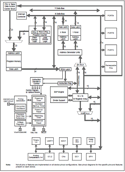
图1。dsPIC33F方框图
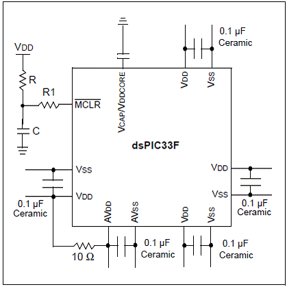
图2。dsPIC33F推荐的最少连接图
A PLM, also referred to as a Power Line Communication (PLC) modem, uses the existing power lines to provide a cost-effective communication medium. This technology can be used for a wide range of applications including, but not limited to, Automated Meter Reading (AMR), energy consumption monitoring of individual appliances, and lighting, heating, and solar applications. Data rate and robustness of a power line communication link are the main parameters that decide its application spectrum.
The Utility-band BPSK 6.0 kbps PLM PICtail™ Plus Daughter Board incorporates Analog
Front End (AFE) circuitry, which is required to implement a software-based modem, using the dsPIC33F Digital Signal Controller (DSC) device on the Explorer 16 Development Board. The daughter board fits into the expansion slot on the Explorer 16 Development Board. A HV adapter cable (included in the package) interfaces the daughter board to the power line. The HV adapter cable incorporates the circuitry required to provide noise-filtering and isolation from the power line. The daughter board and the HV adapter cable are designed to operate at a carrier frequency of 72 kHz (CENELEC-A band).
The daughter board does not implement any particular modulation technique. Software on the dsPIC33F DSC device generates 4-channel PWM output, which when summed-up and filtered suitably by the daughter board circuitry, forms an approximated sine wave. This approximated sine wave is modulated in the software using the BPSK modulation technique by controlling the PWM channels. On the receive path, the modulated signal on the power line is filtered and amplified by the daughter board before being fed to the ADC input of the dsPIC33F DSC device. The ADC module on the dsPIC33F DSC device converts this received signal into the digital domain where further filtering and demodulation is performed in software to recover the data.
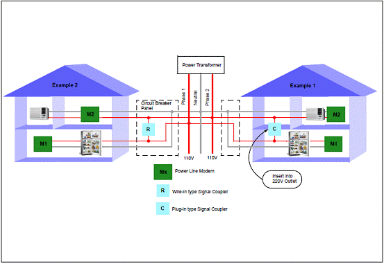
图3。双相电源应用案例
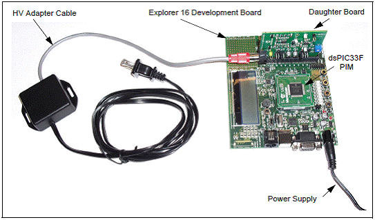
图4。dsPIC33F PLM子板和开发板外形图
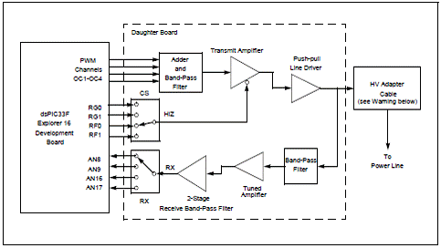
图5。dsPIC33F BPSK 6.0 kbps PLM PICtail+子板框图
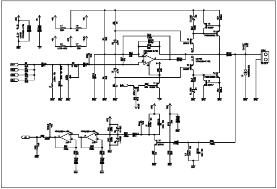
图6。dsPIC33F PLM子板电路图(1)
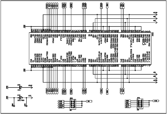
图7。dsPIC33F PLM子板电路图(2)
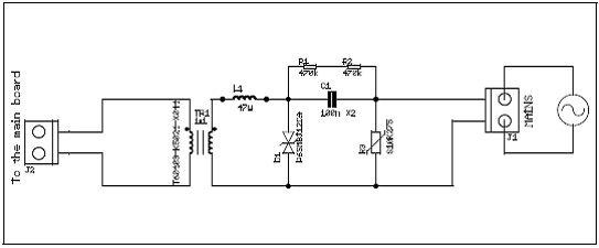
图8。dsPIC33F HV适配器电路图
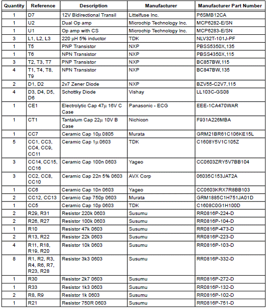
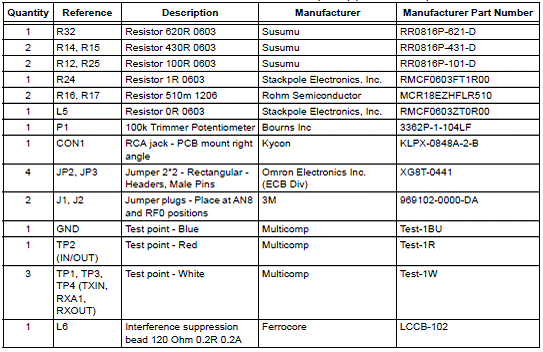
子板材料清单:
HV适配器材料清单(BOM):
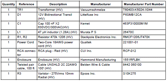
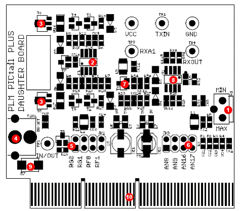
图9。dsPIC33F PLM子板元件布局图
详情请见:
http://ww1.microchip.com/downloads/en/DeviceDoc/70318D.pdf
和
http://ww1.microchip.com/downloads/en/DeviceDoc/DS75019A.pdf