TI TPS62730高频超低功耗DC电源解决方案
2011年08月30日 11:17 发布者:Liming
TI公司的TPS62730是高频超低功耗同步降压DC/DC转换器,非常适合用在低功耗小于1GHz和2.4GHz RF收发器。TPS62730输入电压从1.9V到3.9V,超低功耗旁路模式的功耗为30nA,DC/DC转换器静态电流25uA,开关频率高达3MHz,DC/DC效率高达95%,输出峰值电流高达100mA,主要用在CC2540蓝牙低功耗系统级解决方案,低功耗无线应用和RF4CE表。本文介绍了TPS62730主要特性,功能方框图,典型应用电路以及TPS62730EVM-726评估模块主要特性,电路图和材料清单。The TPS62730 is a high frequency synchronous step down DC-DC converter optimized for ultra low power wireless applications. The device is optimized to supply TI’s Low Power Wireless sub 1GHz and 2.4GHz RF transceivers and System-On-Chip-solutions. The TPS62730 reduces the current consumption drawn from the battery during TX and RX mode by a high efficient step down voltage conversion. It provides up to 100mA output current and allows the use of tiny and low cost chip inductors and capacitors. With an input voltage range of 1.9V to 3.9V the device supports Li-primary battery chemistries such as Li-SOCl2, Li-SO2, Li-MnO2 and also two cell alkaline batteries.
The TPS62730 features an Ultra Low Power bypass mode with typical 30nA current consumption to support sleep and low power modes of TI’s CC2540 Bluetooth Low Energy and CC430 System-On-Chip solutions.
TPS62730主要特性:
Input Voltage Range VIN from 1.9V to 3.9V
Typ. 30nA Ultra Low Power Bypass Mode
Typ. 25 µA DC/DC Quiescent Current
Internal Feedback Divider Disconnect
Typ. 2.1Ω Bypass Switch between VIN and VOUT
Automatic Transition from DC/DC to Bypass Mode
Up To 3MHz switch frequency
Up to 95% DC/DC Efficiency
Open Drain Status Output STAT
Output Peak Current up to 100mA
Fixed Output Voltage 2.1V
Small External Output Filter Components 2.2µH/ 2.2µF
Optimized For Low Output Ripple Voltage
Small 1 × 1.5 × 0.6mm3 SON Package
12 mm2 Minimum Solution Size
TPS62730应用:
CC2540 Bluetooth Low Energy System-On-Chip Solution
Low Power Wireless Applications
RF4CE, Metering
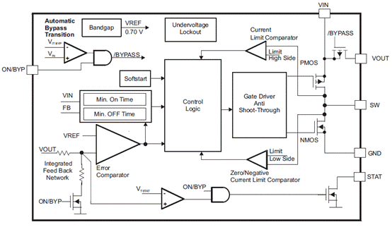
图1。TPS62730功能方框图
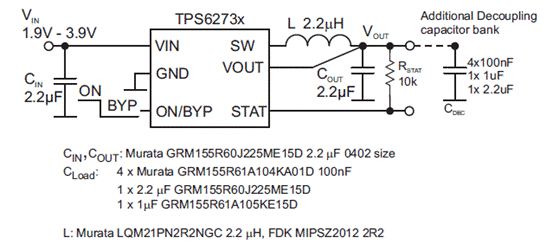
图2。TPS62730典型应用电路图
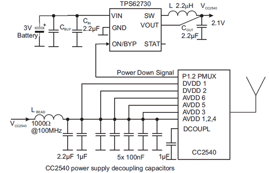
图3。TPS62730用于CC2540的电路图
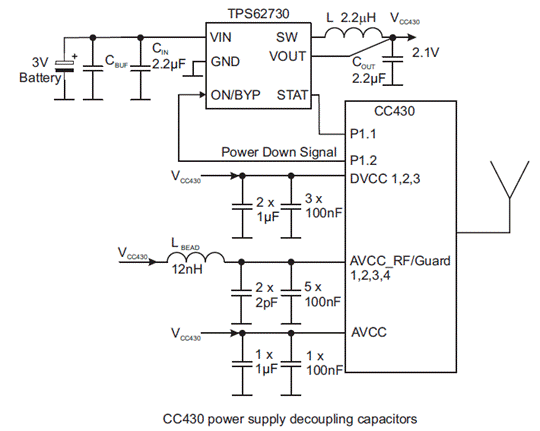
图4。TPS62730用于CC430的电路图
TPS62730EVM-726评估模块
The TPS62730EVM-726 evaluation module (EVM) helps designers evaluate the operation and performance of the TPS62730 step-down converter. The user’s guide describes the TPS62730 evaluation module, how to perform a stand-alone evaluation or interface with a host or system. The converter is designed to deliver up to 100 mA of continuous current to the output. The converter can be switched into bypass mode by grounding the ON/BYP pin or automatically with the input voltage falling to the output regulation voltage. The TPS62730 device is a high-frequency synchronous stepdown dc-dc converter optimized for ultralow-power wireless applications. The device is optimized to supply TI’s low-power wireless sub-1-GHz and 2.4-GHz RF transceivers. The TPS62730 reduces the current consumption drawn from the battery during TX and RX modes by a highly efficient stepdown voltage conversion. It provides up to 100-mA output current and allows the use of tiny and low-cost chip inductors and capacitors. This device supports most Li-ion primary battery chemistries, with an input range of 1.9 V to 3.9 V dc. The TPS62730 features an ultralow-power bypass mode with a typical 30 nA current consumption to support low-power modes of modern RF transceivers. In this bypass mode, the input is connected the VOUT pin via an internal 2-Ω bypass FET. The device automatically enters bypass mode when the input (battery) voltage falls to the bypass transition threshold.
TPS62730EVM-726评估模块主要特性:
Input Voltage Range V IN from 1.9V to 3.9V
Typ. 30nA Ultra Low Power Bypass Mode
Typ. 25 µA DC/DC Quiescent Current
Internal Feedback Divider Disconnect
Typ. 2.5Ω Bypass Switch between V IN and VOUT
Automatic Transition from DC/DC to Bypass Mode
Up To 3MHz switch frequency
Up to 95% DC/DC Efficiency
Open Drain Status Output STAT
Output Peak Current up to 100mA
Fixed Output Voltage Options 2.1V, 2.05V and 1.9V
Small External Output Filter Components 2.2µH/ 2.2µFv
Optimized For Low Output Ripple Voltage
Small 1 × 1.5 × 0.6mm3 SON Package
12 mm2 Minimum Solution Size
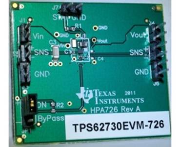
图5。TPS62730EVM-726评估模块外形图
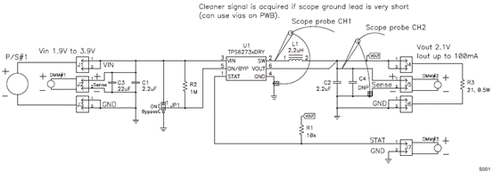
图6。TPS62730EVM-726评估模块电路图和建立图
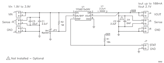
图7。TPS62730EVM-726评估模块电路图
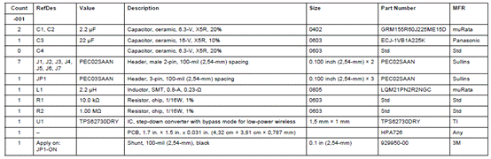
TPS62730EVM-726评估模块材料清单:
详情请见:
http://focus.ti.com/lit/ds/symlink/tps62730.pdf
和
http://focus.ti.com/lit/ug/slvu455/slvu455.pdf
网友评论
1770309616 2011年09月27日
详情请见:
详情请见:
正在招聘电源工程师岗位,要求:1、本科及以上学历,电力电子、电气工程、自动控制等相关专业;
2、3年以上通信电源产品设计经验,能独立从事通信电源产品的研发与设计;
3、有较强地独立分析、解决电源调试及工程应用问题的能力;
4、熟悉功率半导体器件、磁性元器件选型应用,熟悉电源产品可靠性设计;
5、能熟练阅读和理解电力电子专业相关的英文资料,具有良好的团队意识和协作精神;
工作地点:上海张江,有意者请发简历到:vickyyang9936@gmail.com,薪资给力!